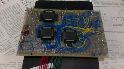
Final CPLD in Place!
I successfully programmed the verilog for the GPIO/SPI chip into the CPLD and popped it into place. Next step is to wire it up and use the flash programmer bus controller to see if I can control GPIO, read GPIO, and use the SPI bus.
Here is a picture with all three CPLDs in place:
It is the one in the upper left.
The pin assignments section from the .lco file that I will use to wire it in. I’ll start with A7:0, D7:0, RD , WR , and IORQ . Also CLK to the simulated CLOCK from the Arduino.
 1 [LOCATION ASSIGNMENTS]
 2 Layer = OFF;
 3 pins_A_7_ = pin,20,-,B,-;
 4 pins_D_7_ = pin,2,-,A,-;
 5 pin_CLK = pin,11,-,-,-;
 6 pin_nRESET = pin,16,-,B,-;
 7 pin_nIORQ = pin,15,-,B,-;
 8 pin_nRD = pin,27,-,C,-;
 9 pin_nWR = pin,14,-,B,-;
10 pin_Din = pin,29,-,C,-;
11 pins_A_6_ = pin,9,-,A,-;
12 pins_A_5_ = pin,7,-,A,-;
13 pins_A_4_ = pin,5,-,A,-;
14 pins_A_3_ = pin,33,-,-,-;
15 pins_A_2_ = pin,21,-,B,-;
16 pins_A_1_ = pin,17,-,B,-;
17 pins_A_0_ = pin,18,-,B,-;
18 pins_D_6_ = pin,25,-,C,-;
19 pins_D_5_ = pin,31,-,C,-;
20 pins_D_4_ = pin,36,-,D,-;
21 pins_D_3_ = pin,4,-,A,-;
22 pins_D_2_ = pin,26,-,C,-;
23 pins_D_1_ = pin,41,-,D,-;
24 pins_D_0_ = pin,43,-,D,-;
25 pins_GPIO_7_ = pin,6,-,A,-;
26 pin_Dout = pin,19,-,B,-;
27 pin_SCK = pin,3,-,A,-;
28 pins_GPIO_6_ = pin,24,-,C,-;
29 pins_GPIO_5_ = pin,28,-,C,-;
30 pins_GPIO_4_ = pin,42,-,D,-;
31 pins_GPIO_3_ = pin,8,-,A,-;
32 pins_GPIO_2_ = pin,30,-,C,-;
33 pins_GPIO_1_ = pin,39,-,D,-;
34 pins_GPIO_0_ = pin,37,-,D,-;