Connections Soldered In. Power Wires Layed
A got the conections all soldered in. I shortened the lead length to 5 holes (0.5”) and realized that I didn’t have to strip both ends, just one end and slide the insulation. Still it takes about 2 hours to solder one 44 PLCC with its connections. Then another close to an hour to bend and lay in the power which I haven’t soldered in yet.
I also did a continuity check between the socket interior and the pins of the header. As well as tested for shorts. Everything is OK.
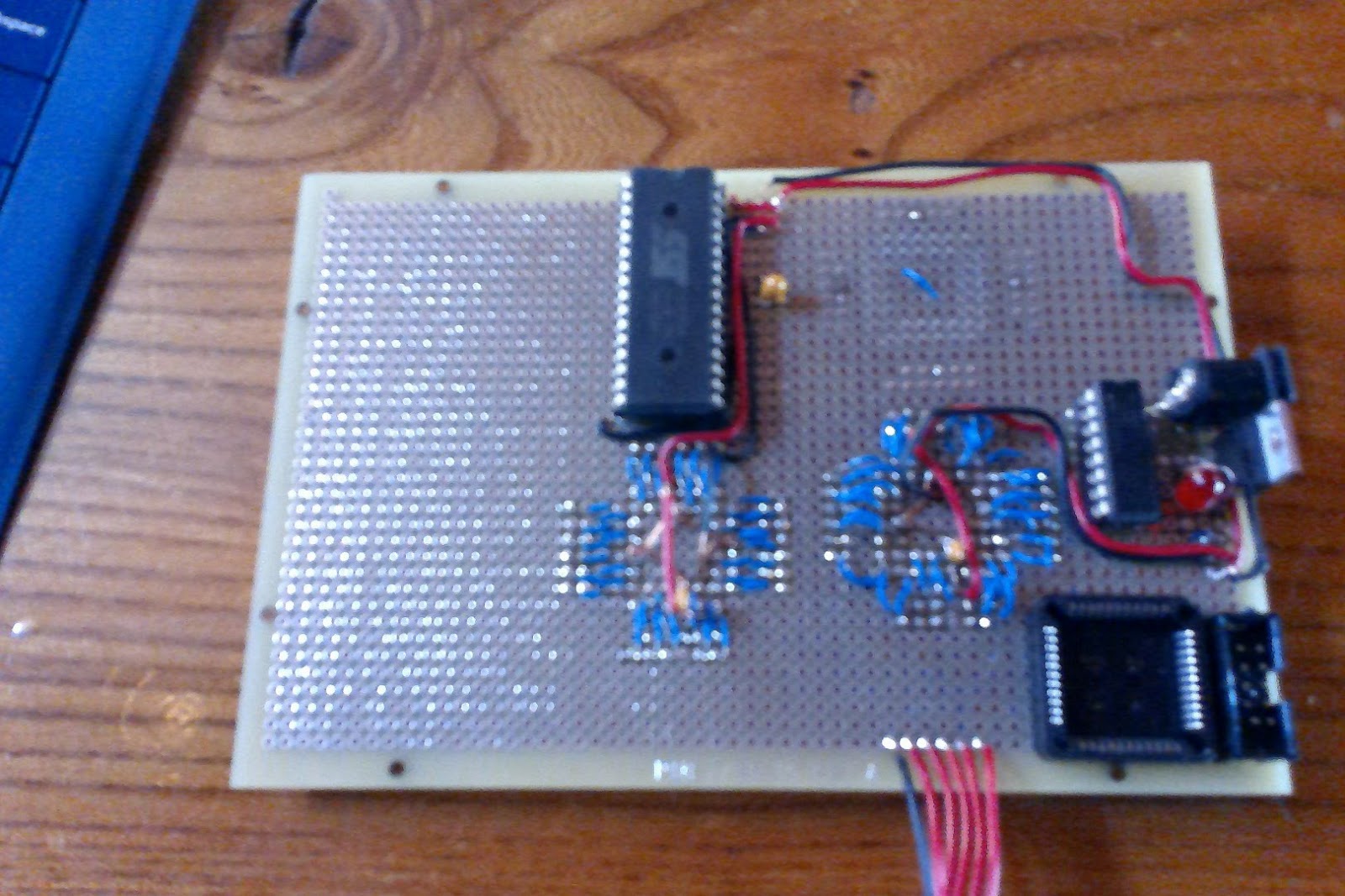
Here is a bit of a blurry picture of the board (I’m at a cafe and don’t have my usual lenses).
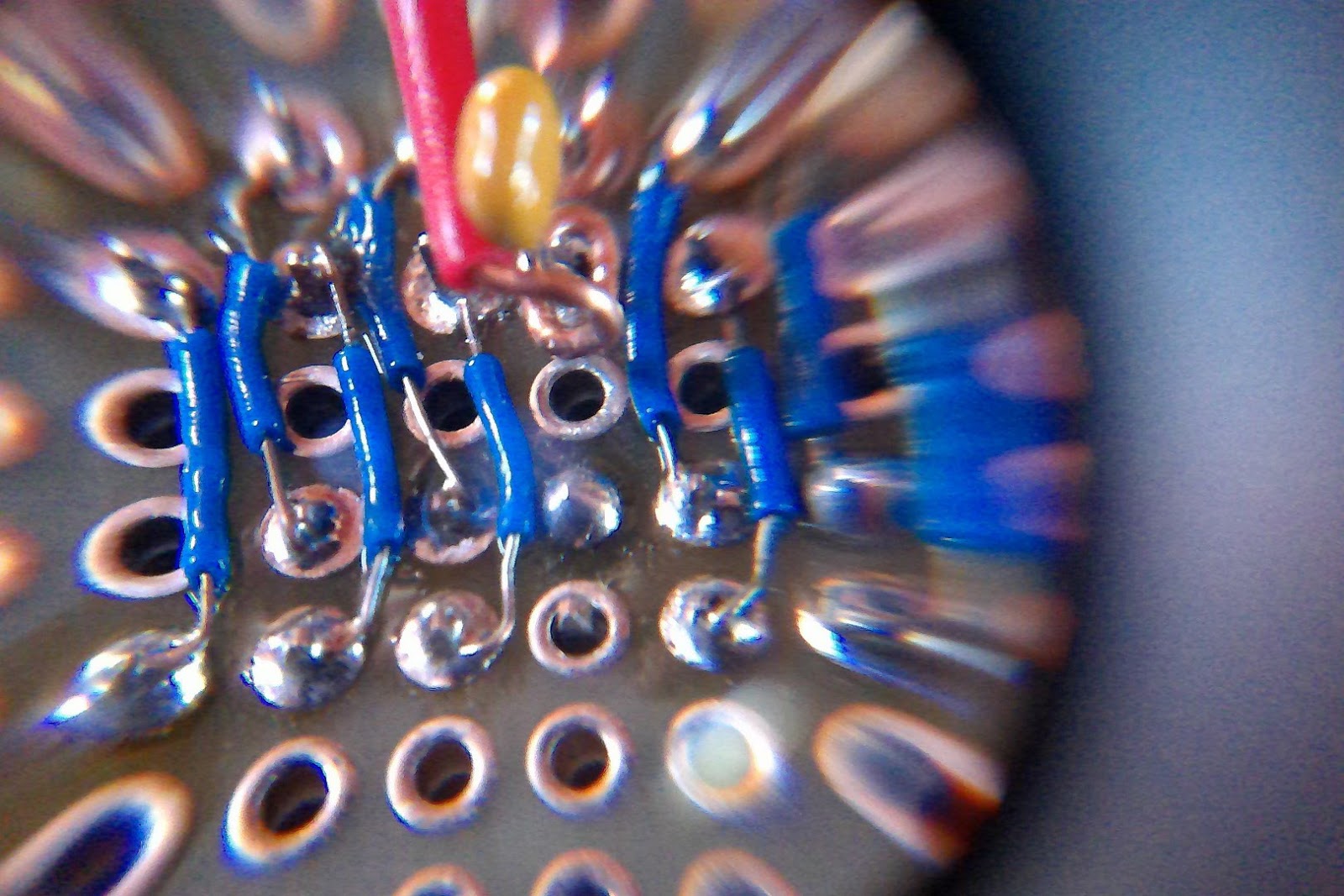
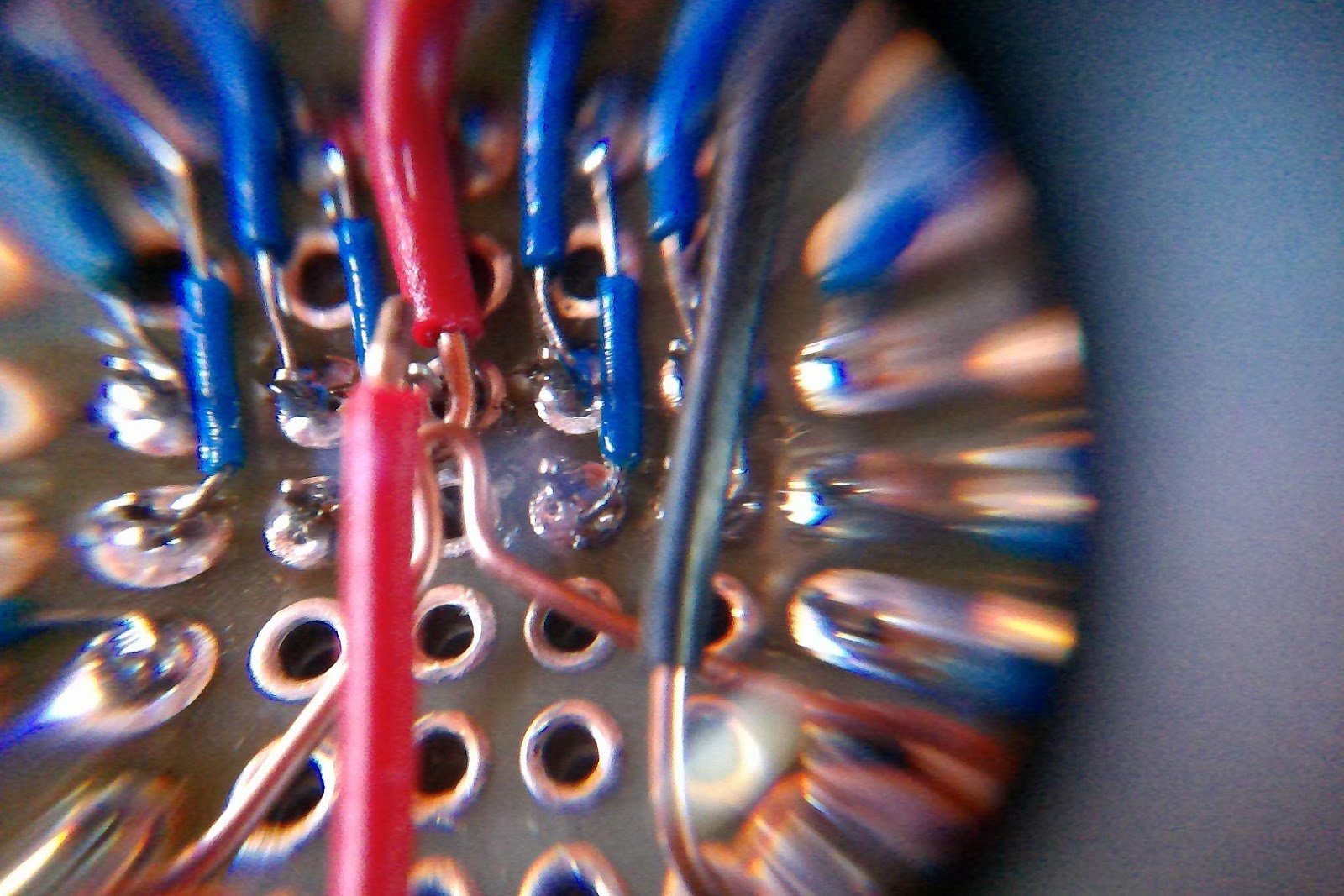
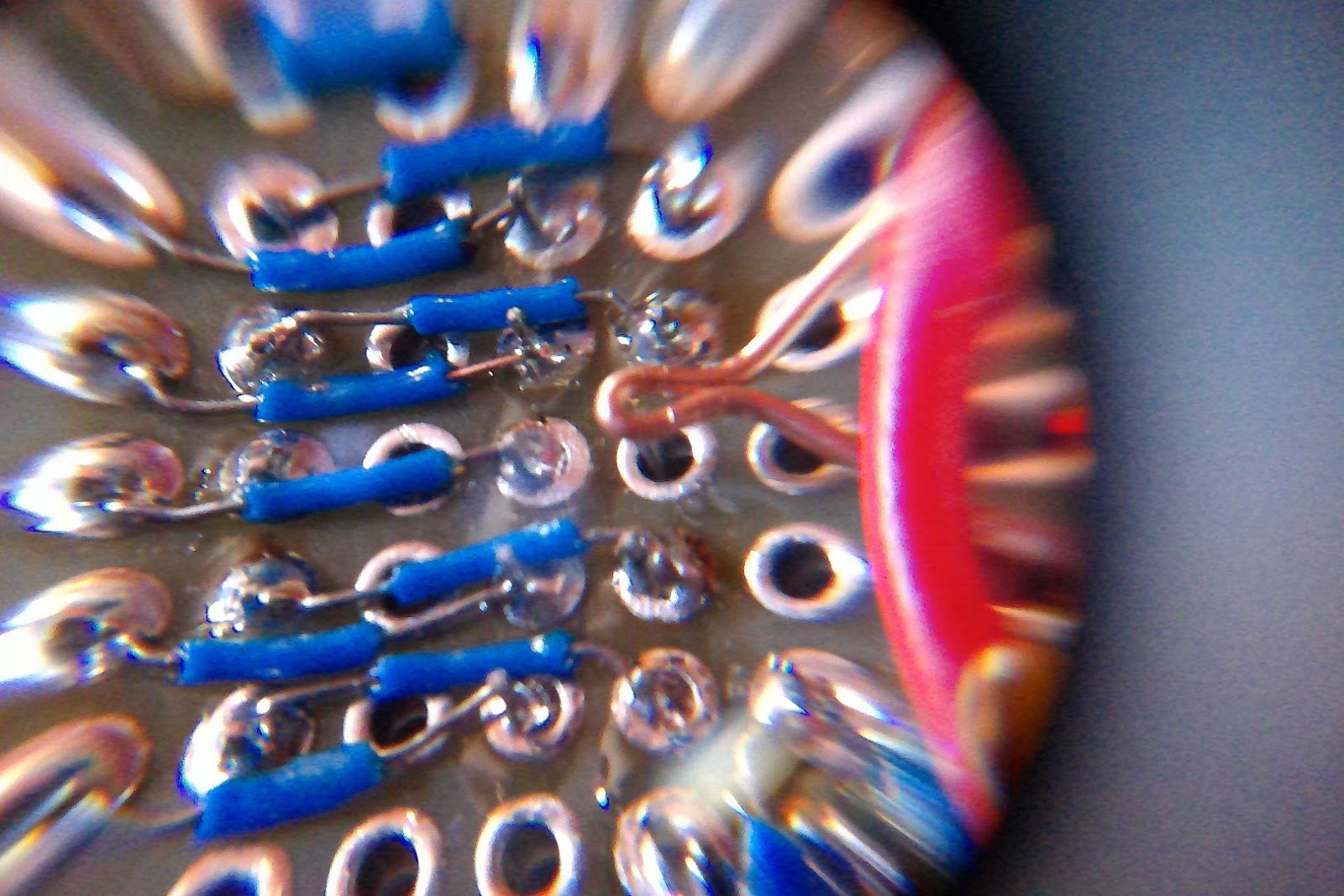
Loupe closeups on the four sides:

This will hold the memory bank switcher. Once this is in, it will be safe to put the SRAM and CPU in without fear of bus contention. I also have to make sure that the in-circuit flash programmer is properly connected so that it doesn’t drive the bus while the CPU is. I’m thinking I’ll run the enable line of the Arduino flash programmer to BUSREQ on the Z-80 and then BUSACK to the CPLD ENABLE line. Then the flash programmer can only ever be enabled when the CPU is not driving the bus.