Some Design, Some Work, Some...Success
I made some 8.5” x 14” sheets of my notebook page to plan my routing. Here are two sheets that show some of what I plan to do tonight.
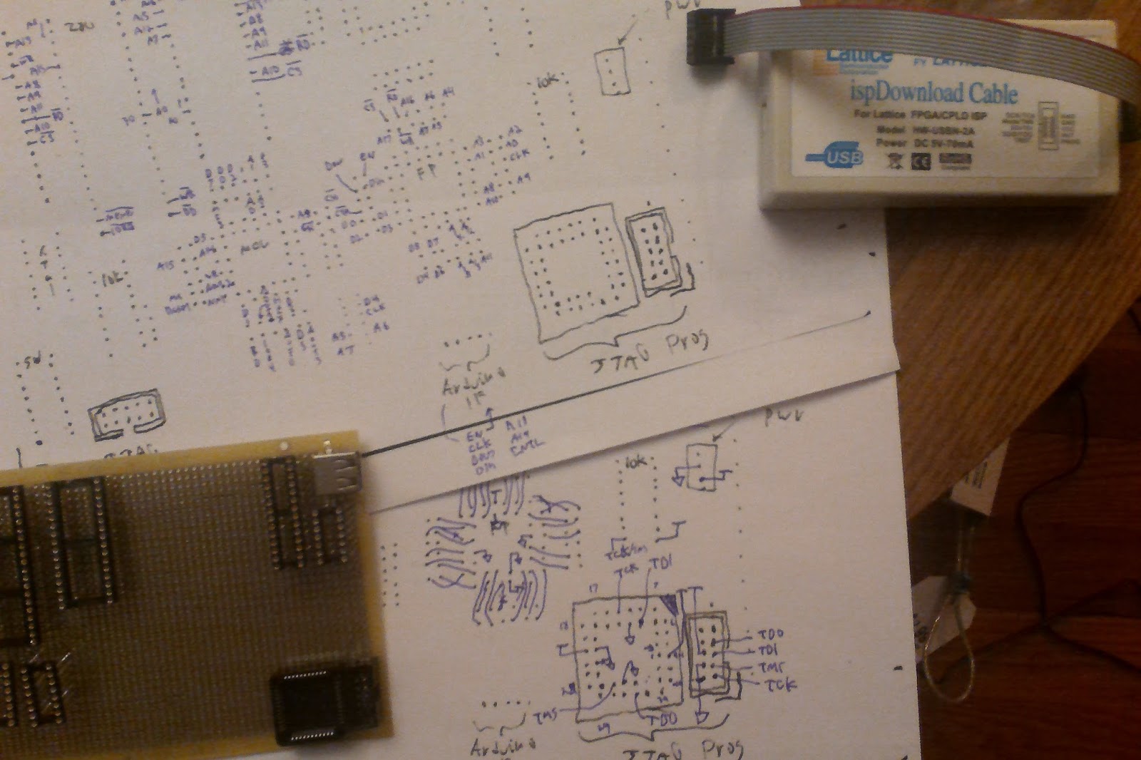
So, let me explain what this is. The top sheet shows the address lines according to location on the PCB. (Yes, I know that it’s not really a “printed” circuit board, but I still call it a PCB in my head.) The bottom sheet shows the design for the dedicated JTAG programmer. The lower left of the PCB shows that dedicated programmer PLCC-44 socket and the 2x5 pin header for the JTAG connecter. The ispDownload Cable in the upper right of the picture is my Lattice JTAG programmer.
I’ll also place the 5V voltage regulator in the space just above the dedicated JTAG programmer. Which is important because that’s the first thing I’ll do. Make sure I can generate a 5V power supply.
I’ll use the dedicated JTAG programmer to create the flash programmer CPLD. Then I’ll pop it out and place it in a socket that will underneath the PCB. On all 4 sides of the socket I’ll have 12 pin headers that will be wirewrappable connections to the PLCC socket. To connect them together, I’ll solder little wires from the socket pins to the header pins. The little wires are shown in the lower sheet just to the upper left of the dedicated JTAG socket.
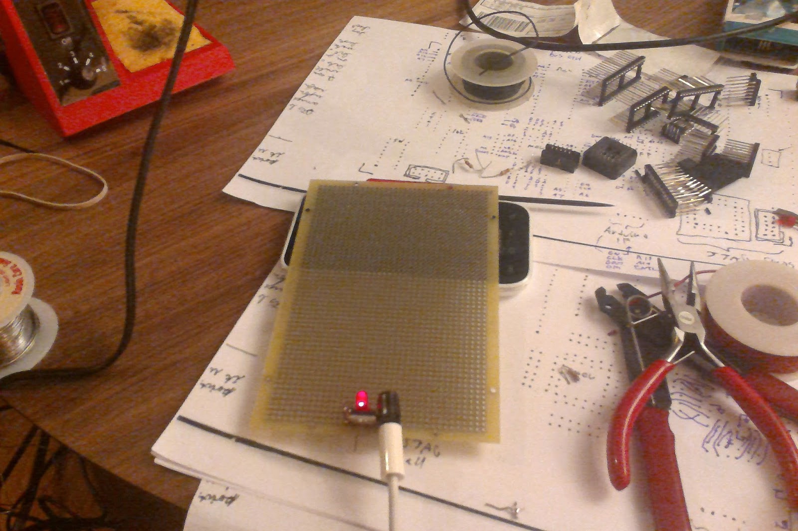
So my nest steps are: solder in the voltage regulator, and an LED/220 ohm resistor plug into a $4 power supply I got from Value Village. ensure the LED lights up.
So—I’ve just done 2/3 of these. I do have a 5V supply, but the diode isn’t lighting up. Also, I suck at soldering. Thank goodness that I have a 10x jeweler’s loop. I think I need magnifying glasses.
I replaced the diode–no small feat for someone who sucks at soldering. And it lights up now!
Yay!!! My first triumph. 5V and a lit up LED!!! I’ll see if my kitchen thermometer can see how hot the voltage regulator is getting….not hot at all.
Here’s proof of the light.