Starting Layout
Thinking about layout.
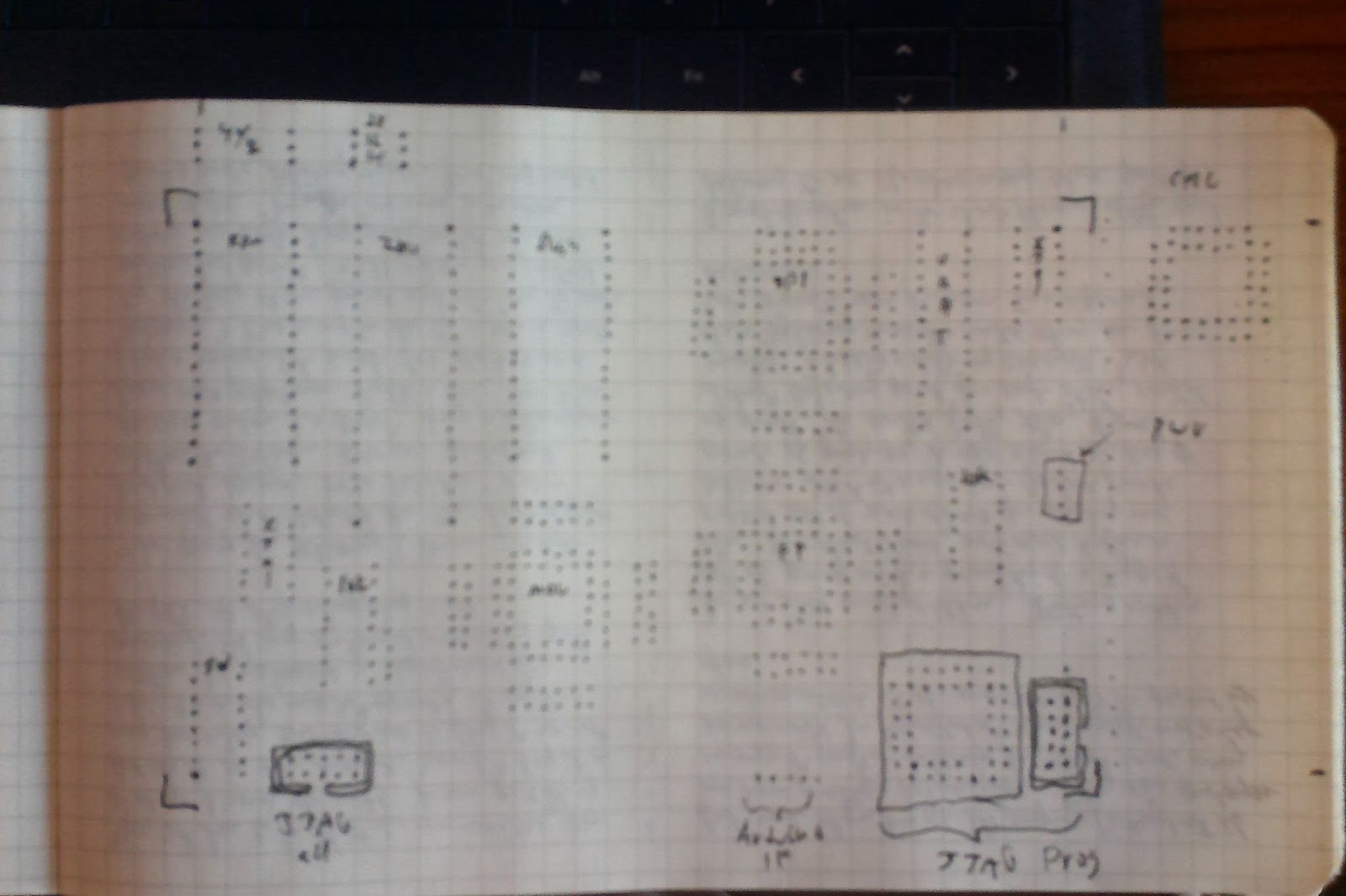
The upper left has the SRAM, Z-80, and flash. The lower left has the DIP switches, 2MHz oscillator, and a 10k resistor net for pullups. The square network under the flash is the socket and headers for the MCU CPLD. The upper right is the UART and oscillator. The lower right is a dedicated hardwired JTAG programming socket. Finally, between the flash and UART are the UART-SPI CPLD (top) and in-circuit flash programmer CPLD (bottom).
Initially, I’ll wire the enable up to the Arduino and control it directly. But once I’m ready, I’ll connect the Arduino to the Z-80 BUSREQ pin and then use the BUSACK to set enable on the flash programmer.
I’ll print off a few blown up copies of this to plan my wire-wrap/soldered wire routes:
- power
- ground
- clock
- bus control
- pullups
- address
- data
- misc